Advancing Precision: How Custom Manufacturing Shapes Numerical Aperture Specifications
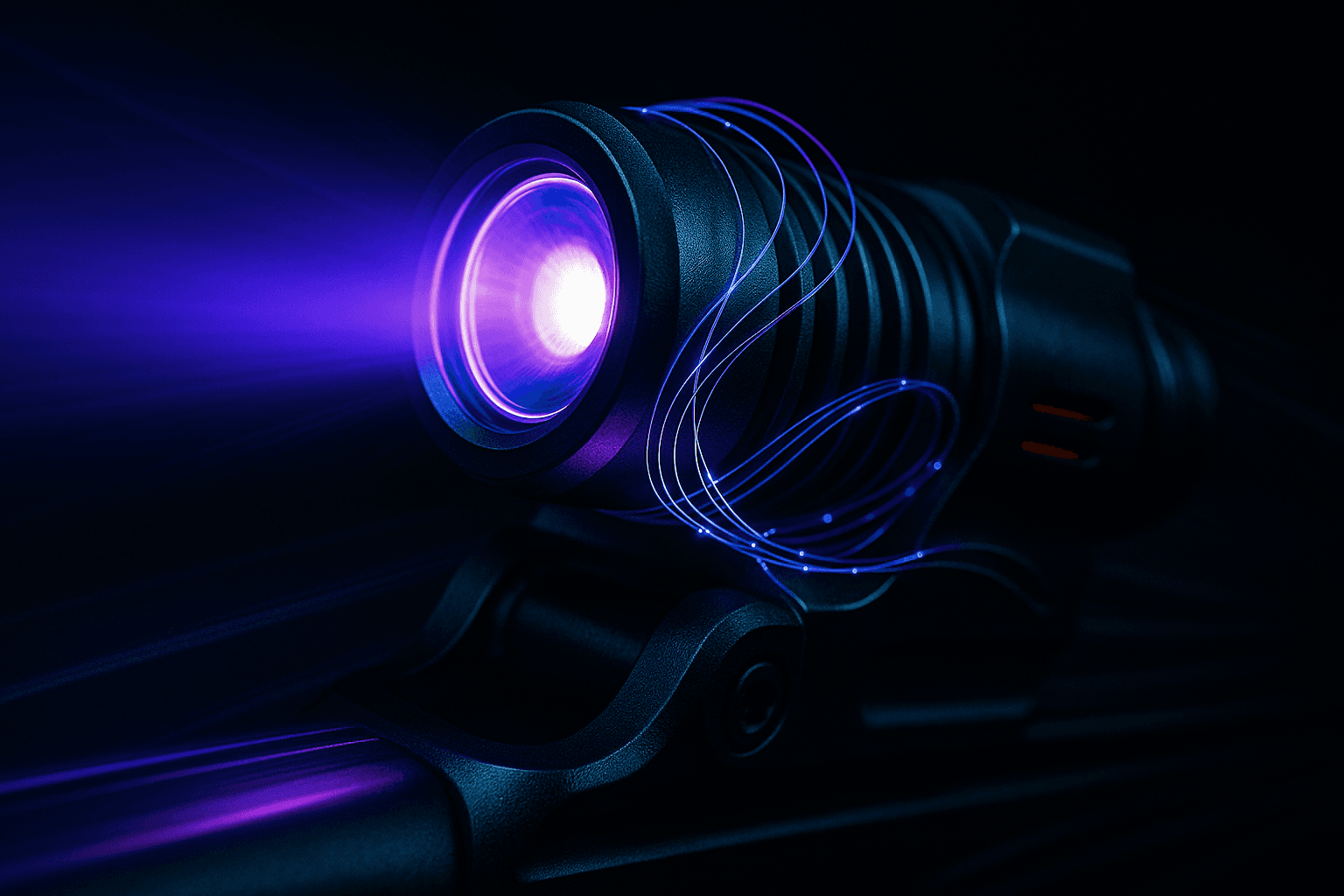
Numerical Aperture (NA) is the cornerstone metric that determines how much light an optical system can collect, how finely it can resolve detail, and how deep its focus extends. In sectors ranging from semiconductor lithography to medical imaging and fiber‑optic data transmission, the ability to control NA with tight tolerances directly translates into performance gains, cost savings, and competitive advantage. Yet NA is not merely a design number; it is a manufacturing challenge that demands specialized processes, rigorous metrology, and cross‑disciplinary collaboration. This guide explores the technical underpinnings of Numerical Aperture Specifications: Custom Manufacturing Capabilities, outlines the critical steps in the production workflow, and highlights the trade‑offs that engineers must negotiate when pushing NA beyond conventional limits.
Understanding Numerical Aperture and Its Systemic Impact
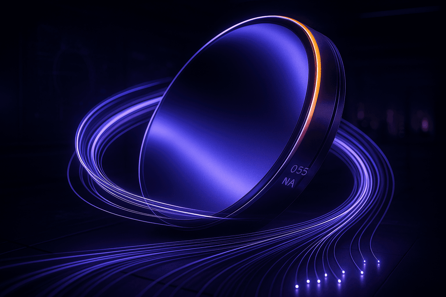
At its most basic, numerical aperture is defined as NA = n · sin θ, where n is the refractive index of the medium surrounding the aperture and θ is the half‑angle of the maximum cone of light that can enter or exit the system. A higher NA enlarges this cone, allowing more light to be captured and enabling finer resolution according to the Rayleigh criterion (Δ ≈ 0.61 λ/NA). However, increasing NA also compresses depth of focus (DOF ≈ λ/(2 NA²)) and intensifies sensitivity to aberrations, surface errors, and alignment tolerances.
Because NA simultaneously influences resolution, throughput, and tolerance budgets, any deviation from the intended Numerical Aperture Specifications: Custom Manufacturing Capabilities can cascade into system‑level failures. In high‑volume manufacturing environments, a 0.2 % deviation in NA may translate into yield losses exceeding 10 % for semiconductor masks or signal‑to‑noise penalties in fiber‑optic links. Therefore, the manufacturing ecosystem must be engineered to deliver NA with sub‑nanometer surface accuracy for bulk optics and sub‑percent index uniformity for specialty fibers.
Key Drivers Behind Custom Manufacturing for High NA
Material Purity and Homogeneity: Glass formulations for high‑NA lenses require precise control of dopant concentrations (e.g., lanthanum, titanium) to achieve the desired refractive index without introducing absorption or scattering centers.
Surface Figure and Roughness: For NA values above 0.5, surface irregularities larger than 0.1 µm can degrade modulation transfer function (MTF) and introduce wavefront error beyond λ/20, which is unacceptable for diffraction‑limited performance.
Coating Uniformity: Anti‑reflective and high‑reflective coatings must maintain thickness uniformity within ±1 nm across apertures exceeding 300 mm to prevent NA‑related phase shifts.
Geometric Tolerances: Aspheric and free‑form surfaces used to correct higher‑order aberrations require machining tolerances tighter than ±0.5 µm, especially at the periphery where NA is highest.
Environmental Stability: Thermal expansion coefficients must be matched to system substrates; otherwise, NA drifts with temperature, undermining focus stability in applications such as EUV lithography.
Custom Manufacturing Capability #1: Ultra‑Precision Polishing
The polishing stage is where Numerical Aperture Specifications: Custom Manufacturing Capabilities intersect with nanometer‑scale surface engineering. Modern ion‑beam figuring (IBF) and magnetorheological finishing (MRF) can remove material at rates as low as 0.01 nm/min, enabling the attainment of surface figure errors below 0.02 λ RMS across diameters up to 500 mm. These techniques are essential for high‑NA EUV scanner mirrors, where a 0.55 NA asphere must maintain a peak‑to‑valley error under 2 nm to avoid pattern distortion on the wafer.
Custom Manufacturing Capability #2: Tailored Preform Fabrication for High‑NA Fibers
In fiber optics, NA is primarily governed by the core‑cladding index contrast (Δn). Achieving NA ≈ 0.6 requires a Δn of roughly 0.02–0.025, which can be realized through precise dopant incorporation (e.g., germanium, fluorine) during modified chemical vapor deposition (MCVD) or plasma‑activated chemical vapor deposition (PACVD). Custom preform fabrication facilities employ real‑time spectroscopic monitoring to keep dopant concentration within ±0.5 % over lengths exceeding 1 km. This level of control ensures that the resulting Numerical Aperture Specifications: Custom Manufacturing Capabilities are consistent from spool to spool, reducing splice loss and bend‑induced attenuation.
Custom Manufacturing Capability #3: Integrated Metrology Platforms
Verifying that a component meets its NA target requires a suite of metrological tools:
Interferometric Profilometry: Provides full‑field surface maps for lenses and mirrors, revealing deviations that would affect NA.
Angle‑Resolved Scatterometry: Measures the angular distribution of transmitted or reflected light, directly yielding NA values.
Refractive Index Profiling: Uses optical low‑coherence reflectometry to map index gradients in fibers, confirming NA compliance.
These instruments are typically integrated into a closed‑loop feedback system, allowing manufacturers to adjust polishing or doping parameters on‑the‑fly, thereby tightening the Numerical Aperture Specifications: Custom Manufacturing Capabilities envelope.
Design‑for‑Manufacturability (DfM) Strategies
Even the most advanced manufacturing suite cannot compensate for a design that ignores production realities. DfM principles help align optical performance goals with feasible fabrication routes:
Tolerance Budget Allocation: Distribute NA‑related error budgets across surface figure, coating thickness, and material index, ensuring that no single step dominates risk.
Monte‑Carlo Ray‑Tracing: Simulate the cumulative effect of random manufacturing variations on NA and system MTF, identifying the most sensitive parameters.
Modular Design: Break complex high‑NA assemblies into sub‑components (e.g., lens groups, fiber bundles) that can be independently fabricated and later integrated, reducing overall cycle time.
Prototyping Loops: Use rapid‑prototype polishing or 3‑D printed glass molds to validate NA performance before committing to full‑scale production.
Applying DfM reduces rework, shortens time‑to‑market, and ensures that Numerical Aperture Specifications: Custom Manufacturing Capabilities are realistic and repeatable.
Industry Case Studies Illustrating Custom NA Manufacturing
Case 1: EUV Lithography Mirror Development
A leading semiconductor equipment supplier targeted a 0.55 NA mirror for its next‑generation EUV scanner. By partnering with a custom optics manufacturer that offered in‑house ion‑beam figuring, the project achieved a surface figure of 0.8 nm RMS across a 450 mm aperture. The collaborative workflow—spanning optical design, coating, and metrology—allowed the supplier to meet its NA specification within a 3‑month window, accelerating the scanner’s development schedule by 25 %.
Case 2: High‑NA Fiber Bundle for Endoscopic Imaging
A medical device company required a fiber bundle with NA = 0.58 to deliver sufficient illumination through a sub‑2 mm diameter probe. Custom preform fabrication, combined with real‑time refractive index monitoring, produced a fiber that maintained the target NA over 500 m of draw. The resulting bundle exhibited a 12 % increase in signal‑to‑noise ratio compared with off‑the‑shelf alternatives, directly improving image clarity for surgeons.
Case 3: Aerospace Laser Communication Terminal
A defense contractor needed a free‑form lens with NA = 0.45 to focus a high‑power laser onto a compact detector array. The lens was fabricated using ultra‑precision diamond turning followed by MRF polishing. Integrated interferometric feedback ensured that the final NA matched the design within ±0.003, enabling a 30 % boost in link margin under atmospheric turbulence conditions.
Balancing Performance, Cost, and Risk
When specifying Numerical Aperture Specifications: Custom Manufacturing Capabilities, engineers must weigh three interdependent factors:
Factor | Impact on NA | Typical Mitigation |
|---|---|---|
Performance | Higher NA improves resolution but reduces DOF. | Employ aspheric correction and adaptive optics. |
Cost | Custom polishing, specialized coatings, and tight tolerances raise unit cost. | Leverage batch processing and modular designs. |
Risk | Manufacturing variability can cause NA drift. | Integrate closed‑loop metrology and DfM analysis. |
Strategic trade‑offs often involve selecting a slightly lower NA to gain robustness against environmental fluctuations, especially in field‑deployed systems where temperature control is limited.
Future Directions in Custom NA Manufacturing
Emerging technologies promise to expand the envelope of Numerical Aperture Specifications: Custom Manufacturing Capabilities:
Freeform Additive Glass Printing: Enables complex geometries that traditional grinding cannot achieve, potentially raising NA without additional lens elements.
Meta‑Surface Coatings: Engineered sub‑wavelength structures can tailor effective refractive indices, offering new pathways to high NA with reduced bulk material.
AI‑Driven Process Control: Machine‑learning algorithms analyze real‑time metrology data to predict and correct NA drift before it manifests in final parts.
These advances will further blur the line between design and manufacturing, making the seamless delivery of high NA a standard expectation rather than a niche capability.
Brand Context: Fiberoptic Systems, Inc. (FSI)
Fiberoptic Systems, Inc. (FSI) exemplifies how a focused, privately held organization can leverage Numerical Aperture Specifications: Custom Manufacturing Capabilities to serve demanding markets. Since its founding in 1982, FSI has maintained an in‑house fiber drawing tower, precision polishing bays, and a dedicated metrology suite, allowing the company to produce both standard and highly customized NA‑optimized products. Whether delivering ultra‑high‑NA fibers for medical imaging, bespoke lens assemblies for aerospace telemetry, or ruggedized bundles for defense communications, FSI’s end‑to‑end process ensures that NA performance aligns tightly with client specifications. This integrated approach reduces lead times, minimizes supply‑chain risk, and reinforces FSI’s reputation as a “deep bench” partner for industries where optical performance cannot be compromised.